Before the next generation of GPUs, high-bandwidth memory, and AI accelerators ever reach a data center, they have to be manufactured with extraordinary precision.
One of the most important technologies enabling that process is Extreme Ultraviolet (EUV) lithography). EUV lithography is a critical technology used to manufacture the most advanced semiconductor chips, allowing manufacturers to create increasingly small and complex features on silicon.
As the AI buildout continues to accelerate, the importance of the companies providing the equipment and technology required to manufacture advanced semiconductors is becoming increasingly apparent.
The PurePlay NVIDIA Ecosystem Picks & Shovels Index ETF (NASDAQ: NVPS) is designed to provide exposure to companies across this broader ecosystem, including semiconductor manufacturing and the tools that enable the production of increasingly advanced chips.
[Explore the NVPS Prospectus and Current Holdings Here]
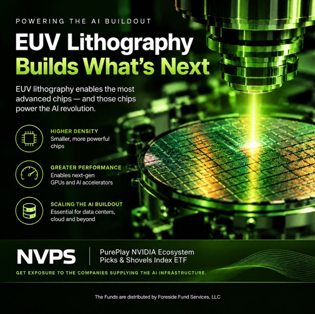
What Is EUV Lithography?
At a basic level, lithography is the process used to transfer extremely detailed circuit patterns onto a semiconductor wafer.
Think of it as a highly sophisticated form of printing. Instead of printing ink onto paper, lithography systems project incredibly precise patterns onto a silicon wafer that ultimately become the circuitry inside a semiconductor.
As chips become more powerful, manufacturers need to fit more transistors into increasingly small areas. That requires the ability to create smaller and more intricate patterns on the wafer.
This is where EUV becomes particularly important.
EUV lithography uses extremely short-wavelength ultraviolet light to create some of the smallest features required for the production of today's most advanced semiconductors. The technology allows chip manufacturers to continue shrinking transistor dimensions while increasing the complexity and performance of the chips they produce.
The machines required to perform this process are among the most sophisticated pieces of manufacturing equipment in the world, incorporating advanced optics, precision engineering, specialized light sources, vacuum systems and software.
Why Does EUV Matter for AI?
The AI revolution is ultimately dependent on semiconductor manufacturing.
The GPUs and AI accelerators powering modern AI systems require increasingly advanced semiconductor processes. As demand for computing power increases, chip manufacturers need to produce more powerful processors while continuing to improve performance and efficiency.
That means the ability to manufacture advanced chips at scale becomes increasingly important.
EUV lithography sits directly within that manufacturing process.
The relationship is relatively straightforward:
AI demand → more AI accelerators → more advanced semiconductors → more sophisticated manufacturing → greater importance of advanced lithography.
That makes semiconductor manufacturing equipment an important part of the broader physical infrastructure behind AI.
And it is not just GPUs. The same broader semiconductor manufacturing ecosystem supports many of the components required throughout modern AI infrastructure, including networking chips, processors, memory-related technologies and other advanced computing components.
The Picks-and-Shovels Opportunity
One of the interesting aspects of the AI investment opportunity is that investors don't necessarily have to focus exclusively on the companies designing or selling AI chips.
There is an enormous ecosystem of companies supplying the equipment, components and infrastructure required to produce and deploy those technologies.
These are the "picks and shovels" of the AI buildout.
Lithography is a particularly good example.
The companies developing advanced lithography systems aren't necessarily selling an AI application. Instead, they are providing some of the critical manufacturing technology required to produce the chips that make AI possible.
The same concept extends across the semiconductor supply chain.
Advanced AI systems require semiconductor manufacturing equipment, high-bandwidth memory, advanced packaging, networking, power and cooling infrastructure, data centers and numerous raw materials and components.
This creates a much broader ecosystem behind the AI buildout than the GPUs themselves.
Gaining Exposure Through NVPS
The PurePlay NVIDIA Ecosystem Picks & Shovels Index ETF (NASDAQ: NVPS) is designed to provide exposure to this broader ecosystem surrounding NVIDIA and advanced AI computing.
Rather than investing directly in NVIDIA, NVPS focuses on companies supporting the production, assembly and deployment of the technology required throughout the NVIDIA ecosystem.
The fund's methodology organizes the ecosystem across six areas: Fabrication, Tools, Packaging, Infrastructure, Connectivity and Raw Materials.
Lithography falls within the Tools portion of that ecosystem.
This is important because the AI buildout requires much more than the finished GPU. Before an advanced processor can power an AI data center, it has to move through a highly complex global manufacturing ecosystem.
EUV lithography is one of the technologies helping make that possible.
The Bigger Picture
The AI infrastructure buildout is still in its early stages, and the amount of capital being committed to expanding AI computing capacity is driving demand throughout the semiconductor supply chain.
As AI models become more capable and computing requirements continue to increase, the physical infrastructure supporting those systems will need to scale as well.
That means more advanced chips, more manufacturing capacity, more memory, more networking and more of the equipment required to manufacture these technologies.
EUV lithography is one piece of that much larger puzzle, but it represents an important connection between the demand for AI computing and the physical manufacturing infrastructure required to deliver it.
For investors looking beyond the headline AI companies, the semiconductor equipment ecosystem offers another way to think about the AI buildout.



Investors should consider the investment objectives, risks, charges and expenses carefully before investing. For a prospectus or summary prospectus with this and other information about the Fund, please visit the website at www.pureplayetfs.com. Read the prospectus or summary prospectus carefully before investing.
The Fund is distributed by Foreside Fund Services, LLC. Exchange Traded Concepts, LLC serves as the investment advisor of the Fund. Foreside Fund Services, LLC is not affiliated with Exchange Traded Concepts, LLC or any of its affiliates.
Risk Disclosures:
Investing involves risk, including possible loss of principal. There is no guarantee the Fund will achieve their stated objectives.
New/Smaller Fund Risk. A new or smaller fund is subject to the risk that its performance may not represent how the fund is expected to or may perform in the long term. In addition, new funds have limited operating histories for investors to evaluate and new and smaller funds may not attract sufficient assets to achieve investment and trading efficiencies.
Non-Diversification Risk. The Fund is non-diversified under the 1940 Act, meaning that, as compared to a diversified fund, it can invest a greater percentage of its assets in securities issued by or representing a small number of issuers. As a result, the performance of these issuers can have a substantial impact on the Fund’s performance.
NVIDIA Dependence Risk. Because the Index is designed to provide exposure to companies that have a material commercial relationship with NVIDIA, the Index, and therefore the Fund, is highly sensitive to NVIDIA-specific developments. Actual or perceived adverse events at NVIDIA, including financial distress, demand declines, supply or regulatory disruptions, litigation, reputational harm, strategic shifts, or insolvency, could impair the results and valuations of Index constituents that rely on NVIDIA as a key customer, supplier, or technology partner, leading to material declines and heightened volatility in the Fund.